Electronics Product Design Sevices
About us
PCB Design and Services
Hardware design Support Blog
PCB design
PCB DESIGN
Flex PCB Material and Detail
Aspect Ratio Plating Capability
Annular Ring
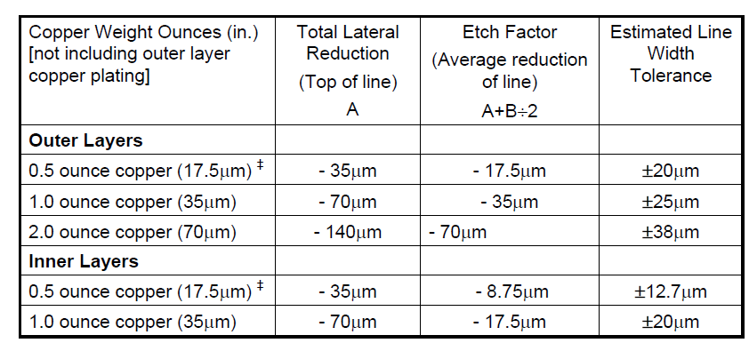
Etch Factor
Expedition Basic
Expedition
Eagle Tool related Issue
Eagle -Copper shape
Eagle PCB Design
EXPEDITION SUPPORT
Flex PCB
Tab Routing
PCB Design Technique
what is the high Speed Board
Flex PCB
How T o Do PCB trace Calculation
TRACE AND SPACE WIDTH Class 3
TRACE AND SPACE WIDTH for Class 1
TRACE AND SPACE WIDTH Class 2
Eagle
Eagle
Flex PCB
Layer selection
PCB Assembly
PCB fabrication
Drill Selection
Through Hole Pads Calculation
PCB fabrication
Electrolytic Capacitor
Eagle PCB Design
EMMC
Standard for automotive
PCB DFM Guideline
Hardware design
I2C
I2C Bus Pullup Resistor Calculation
HOW TO DESIGN BUCK CONVERTER
CAN
NOR FLASH
Motor opration
Power Supply
Component Package information
Capacitor
Ceramic Capacitor
BJT
Bipolar Junction Transistor
Digital Design
Electronics Component
Tantalum Electrolytic Capacitors
CAN differential schematics for High Speed ISO 11898
Complexity Factors Matrix
MOSFET
Popular CAN Physical Layer Standards
EMI-EMC
Uncategorized
Voltage regulator
Uncategorized
Switch
inductor
USB
SPI
LVDS
MICA Capacitor
Relay
NAND FLASH
FLASH
Analog Design
Signal Integrity
Signal Integrity
BIT rate
PPT TO VIDEO
What Are Jitter, Noise, and Signal Integrity
EYE Diagram
SKEW
SDRAM
Signal integrity Issue
Signal Integrity Problem
4 causes of signal integrity issue
Datasheet
Power integrity
Power Integrity
Contact
Online PCB Design and Simulation training
Home
/
Etch Factor
Etch Factor
PCB design
,
PCB fabrication
B. Neem k
May 8, 2020
Advertisements
New Post
Old Post
Advertisements